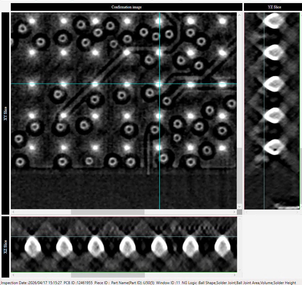
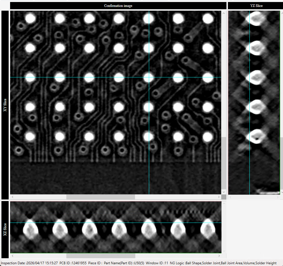
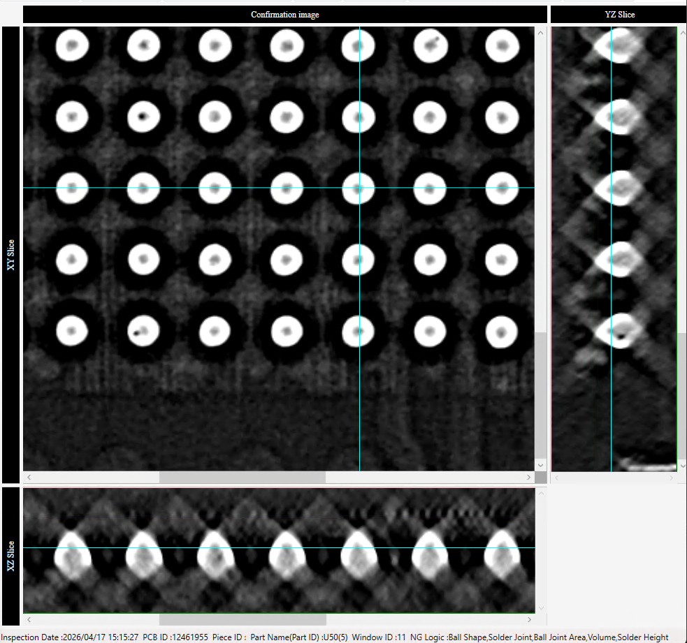
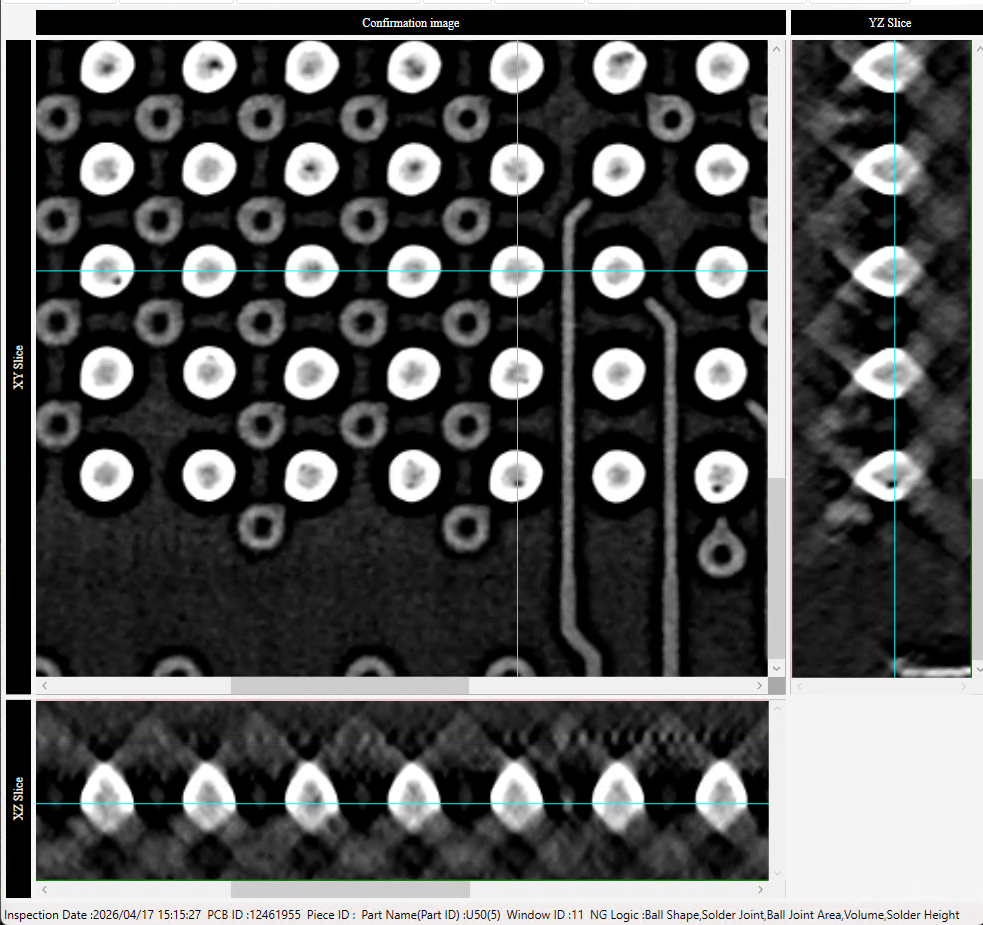
Keytronic, Oakdale MN - X-Ray VT-X750 inspection image help from locked ticket:1707556
CustomerNot indexed
CompanyNot indexed
Priority1
TypeAOI - No Action Required
UpdatedMay 3, 2026 at 3:27 PM
Thread12 messages
Ticket metadata
Group
AOI US (150000419797)
Status
Closed (5)
Created
Apr 20, 2026 at 8:26 AM
Requester
Not indexed
Company
Not indexed
Last synced
Aug 3, 2026 at 12:00 AM
Resolved
Apr 23, 2026 at 11:28 AM
Closed
May 1, 2026 at 3:25 PM
Tags
A - Reply Open, A-REOPEN, LOCKED
Current case
Customer issue
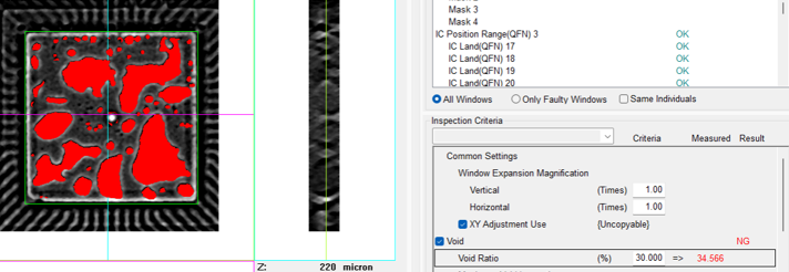
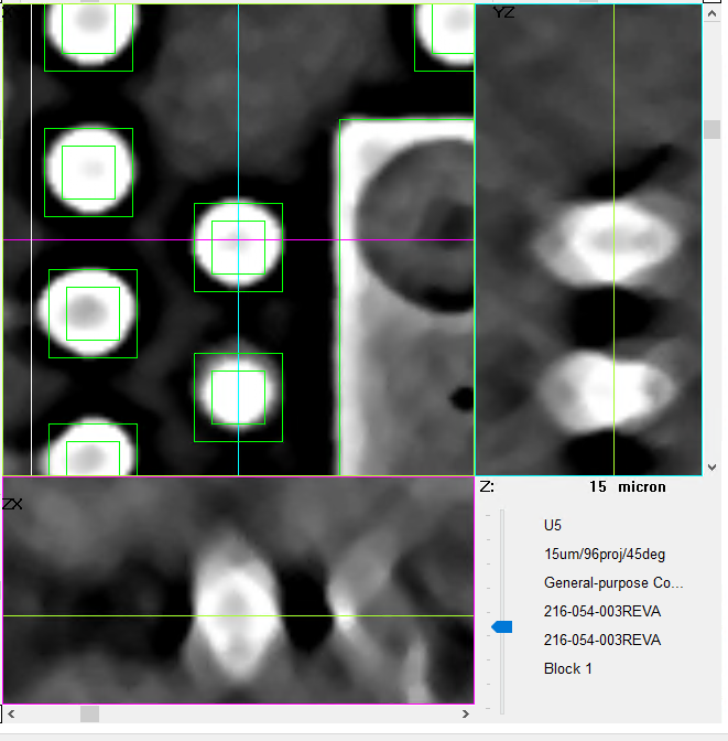
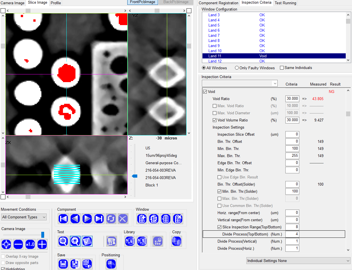
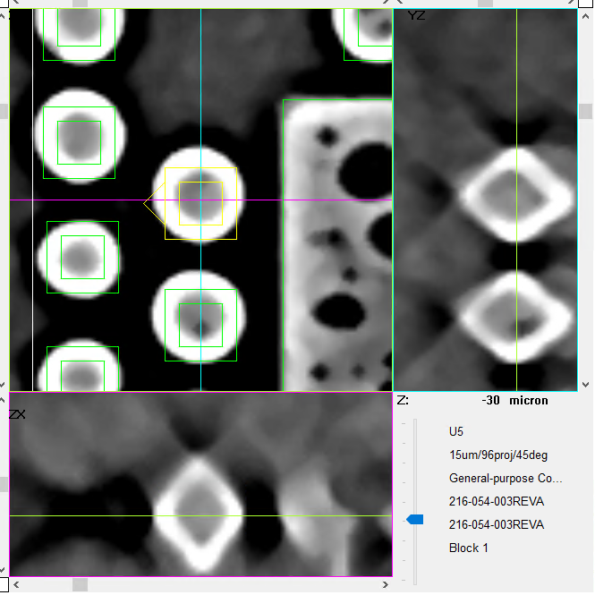
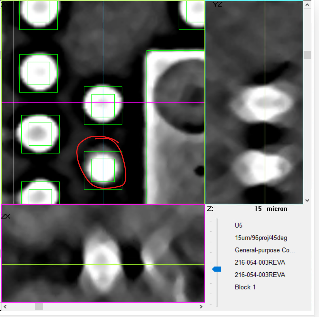
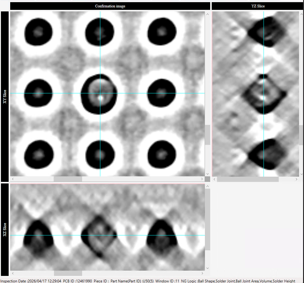
Please check ticket [#{ticket.id}}] for the full message before responding. Last Public comment: Fodor, Tamas : Good morning, I have a BGA with a similar inspection result that I passed acceptable; test failure was the ball is an 'open' connection. Based on the previous information, this was not a defect. Please advise if we are interpreting the grey areas in the x-ray inspection correctly. Tamas Fodor Process Engineer office: [phone] fax: [phone] 7015 55th Street North cell: [phone] Oakdale, MN 55128 [email] keytronic.com From: AOI Tech Support - US Sent: Tuesday, March 3, 2026 09:59 To: Fodor, Tamas Cc: DeMartelaere, Eric ; Dorsey, Callie ; Benson, Andrew Subject: Re: Keytronic, Oakdale MN - X-Ray VT-X750 inspection image help [Case: 1707556] ALERT: This message originated outside of the Keytronic network.BE CAUTIOUS before clicking any link or opening an attachment. Hello Tamas, Gray areas from the previous screenshot should not be considered voids, please adjust Bin Thr in case software is caching it as void. Based on the screenshot you sent, it looks like the issue is different. The ball highlighted in red appears to have a defect, it has a very small connection area and is close to being a HiP. Francisco Villalpando Engineering Supervisor Direct: +[phone] [email] On Tue, 3 Mar at 8:05 AM , Fodor, Tamas wrote: Good morning, Francisco I was waiting on a response for the comparison x-ray image, my initial statement was incorrect about using the same PCB. The LGA PCB footprint, solder paste and oven profile is the same. We will not treat grey areas in solder balls as voids, thank you for your help. Tamas Fodor Process Engineer office: [phone] fax: [phone] mobile: [phone] [email] 7015 55th Street North Oakdale, MN 55128 keytronic.com From: Fodor, Tamas Sent: Thursday, February 26, 2026 10:48 To: AOI Tech Support - US Cc: DeMartelaere, Eric ; Dorsey, Callie ; Benson, Andrew Subject: Re: Keytronic, Oakdale MN - X-Ray VT-X750 inspection image help [Case: 1707556] Francisco, We are using the same part and same PCB on the previous build revision and there is a noticeable difference in the grey areas, it doesn't look like solder to me. Old build x-ray sample: Tamas Fodor Process Engineer office: [phone] fax: [phone] mobile: [phone] [email] 7015 55th Street North Oakdale, MN 55128 keytronic.com From: AOI Tech Support - US Sent: Thursday, February 26, 2026 10:34 To: Fodor, Tamas Cc: DeMartelaere, Eric ; Dorsey, Callie ; Benson, Andrew Subject: Re: Keytronic, Oakdale MN - X-Ray VT-X750 inspection image help [Case: 1707556] ALERT: This message originated outside of the Keytronic network.BE CAUTIOUS before clicking any link or opening an attachment. Hello Tamas, The grey portion of the BGA “style” solder joints are not voids, only the black spots in the image are voids. The outer shell of BGA balls tend to be brighter on larger size balls and darker in middle. If you have smaller ones they generally show up as solid white. Just adjust binarization and test with void ratio overlay to verify. On Thu, 26 Feb at 9:50 AM , Fodor, Tamas wrote: Francisco, Here is an image showing the binarization difference in the balls with grey voids: Tamas Fodor Process Engineer office: [phone] fax: [phone] mobile: [phone] [email] 7015 55th Street North Oakdale, MN 55128 keytronic.com From: AOI Tech Support - US Sent: Thursday, February 26, 2026 08:37 To: Fodor, Tamas Cc: DeMartelaere, Eric ; Dorsey, Callie ; Benson, Andrew Subject: Re: Keytronic, Oakdale MN - X-Ray VT-X750 inspection image help [Case: 1707556] ALERT: This message originated outside of the Keytronic network.BE CAUTIOUS before clicking any link or opening an attachment. Hello Tamas, I replied to your email 2 dasy ago. See below my response Hello Tamas, agree with you—there is only a minimal difference between Reflow 1 and Reflow 2. To determine whether the void percentage is correct, you’ll need to open the program in Teaching Mode and verify that the software is highlighting the voids in red, as shown in the image. If any voids are missing, adjust the Bin. Thr. accordingly. Francisco Villalpando Engineering Supervisor Direct: +[phone] [email] On Thu, 26 Feb at 8:31 AM , Fodor, Tamas wrote: Good morning, We are still waiting for a response on this questions, please advise. Tamas Fodor Process Engineer office: [phone] fax: [phone] mobile: [phone] [email] 7015 55th Street North Oakdale, MN 55128 keytronic.com From: Fodor, Tamas Sent: Tuesday, February 24, 2026 12:50 To: AOI Tech Support - US Cc: DeMartelaere, Eric ; Dorsey, Callie ; Benson, Andrew Subject: Keytronic, Oakdale MN - X-Ray VT-X750 inspection image help Hello, Reaching out for help with interpreting the x-ray inspection image on a LGA. We are noticing some clear voids in the solder balls and some grey areas. Trying to determine if we should treat it as a void, minimal change in the grey areas after a second reflow. X-ray images attached. Tamas Fodor Process Engineer office: [phone] fax: [phone] cell: [phone] [email] 7015 55th Street North Oakdale, MN 55128 keytronic.com This e-mail message may contain confidential or legally privileged information and is intended only for the use of the intended recipient(s). Any unauthorized disclosure, dissemination, distribution, copying or the taking of any action in reliance on the information herein is prohibited. E-mails are not secure and cannot be guaranteed to be error free as they can be intercepted, amended, or contain viruses. Anyone who communicates with us by e-mail is deemed to have accepted these risks. Key Tronic Corporation is not responsible for errors or omissions in this message and denies any responsibility for any damage arising from the use of e-mail. Any opinion and other statement contained in this message and any attachment are solely those of the author and do not necessarily represent those of the company. .
Conversation
Engineer and customer thread
12 messages
OA
Omron Application EngineerOmron reply | Apr 20, 2026 at 10:16 AM
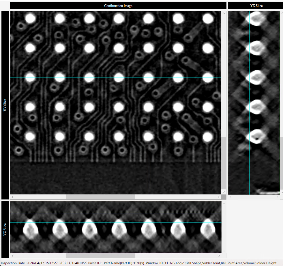
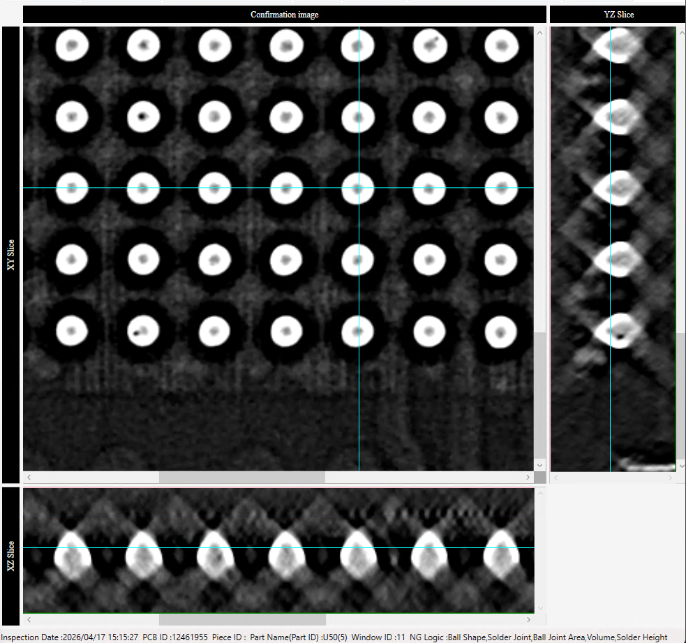
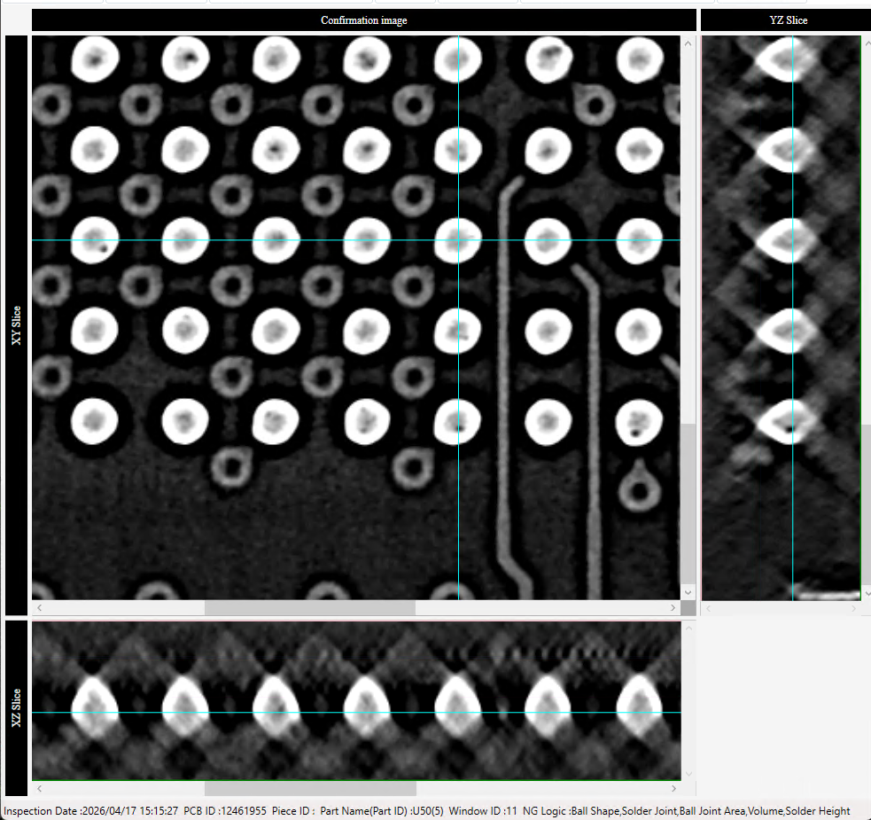
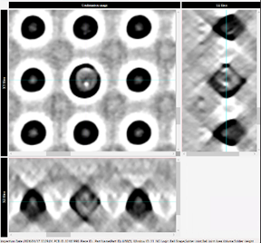
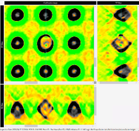
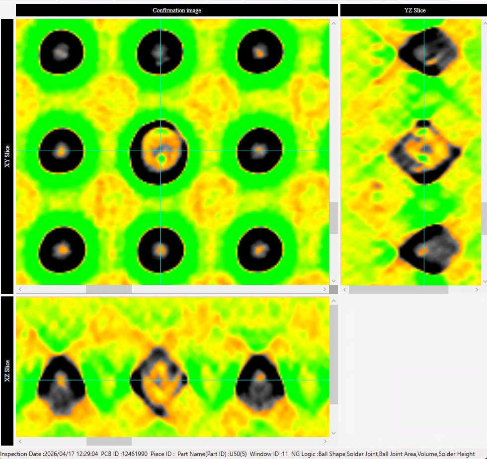
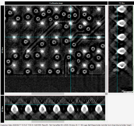
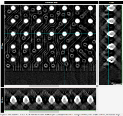
Hello Tamas, I have included your x-ray images and some comments on what I believe is occuring. I hope this is helpful. Am I correct in assuming the at the threshold programmed failed for these solder joint examples? I honestly am not fully sure what the defect is based on the image. I can say that there is a major difference between its shape and size compared to all the surroundings. Barring foreign material mixed into the solder joint (once saw the clear plastic piece from the bare board shipping bag mixed with solder paste and it looked similar). More than likely this could be a HIP. The white center circle may be partially wetting on the pad, with most of the solder volume moving up higher. I would suggest when reviewing this type of solder joint would be to move the horizontal crosshair off the solder joint then very slowly drag the crosshair over the solder joint then look at the side profile x-ray images for two separate masses in the Z. Be sure you do this check and the mid ball and the pad interface slice, the pad region generally shows HIP more clearly. If you see separate masses, it will appear like oval stacked structures, it almost certainly is a defect, it might be electrically ok but will have little to no intermetallic structures. BGA solder joints within the cross hair ok, the one below it either had a BGA ball defect from the manufacture or there was an aperture issue cause less solder paste to be deposited. It looks like it is making electric contact, for structural analysis you would need to move the slice downwards into the pad interface region to truly know. Looking at the difference between these two images I believe I can explain the cause. Look at the thermal pad in this image, there is a large void in the upper left corner. It causes the component to lift off the board in turn causing the solder joint to elongate and thin across many balls, the smallest one had a solder volume issue then also got stretched. The image on the right side is likely to have the opposite side of the thermal pad with voids; this side component is getting slightly flattened. Thus, causing the diameter of solder joint to be massive. In some case nearly large enough to violate min. electrical clearance. As mentioned in the comment on the left component I believe the component is leaned onto this side of the component thus compressing the solder joints. The large grey center area is primary the result of the 45° angle the CT is captured, there may be some in minor density changes in the structure of the solder, but it again mostly the result of CT. Now within the grey area are small consistence black areas, this is 100% flux gas void stuck in the solder joint.
C
CustomerCustomer reply | Apr 20, 2026 at 11:10 AM
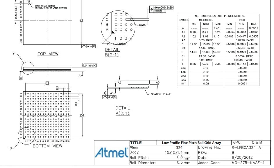
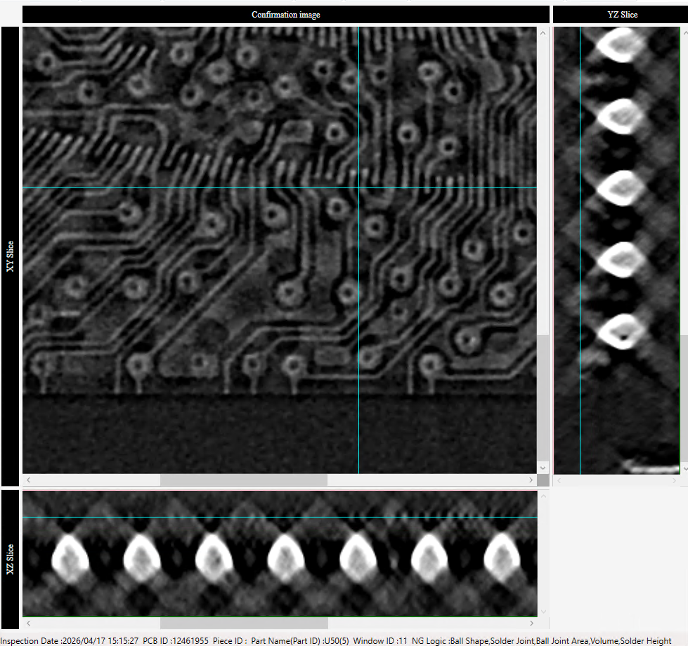
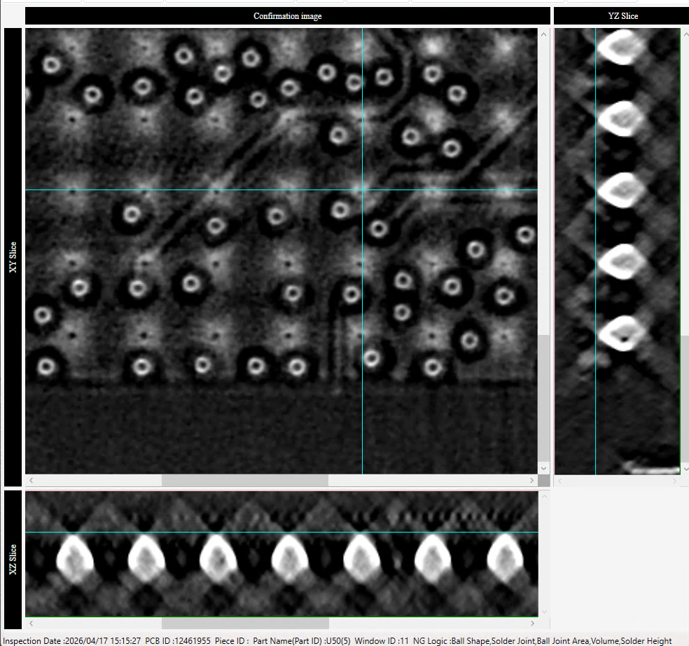
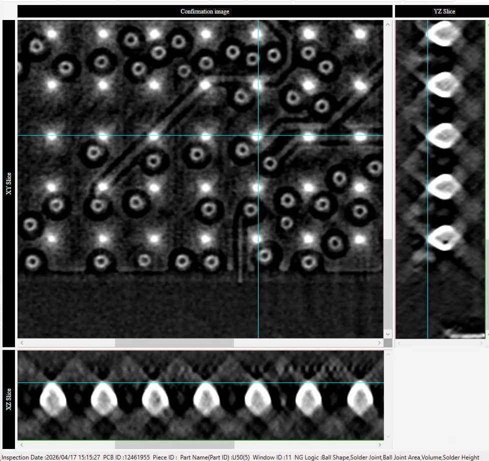
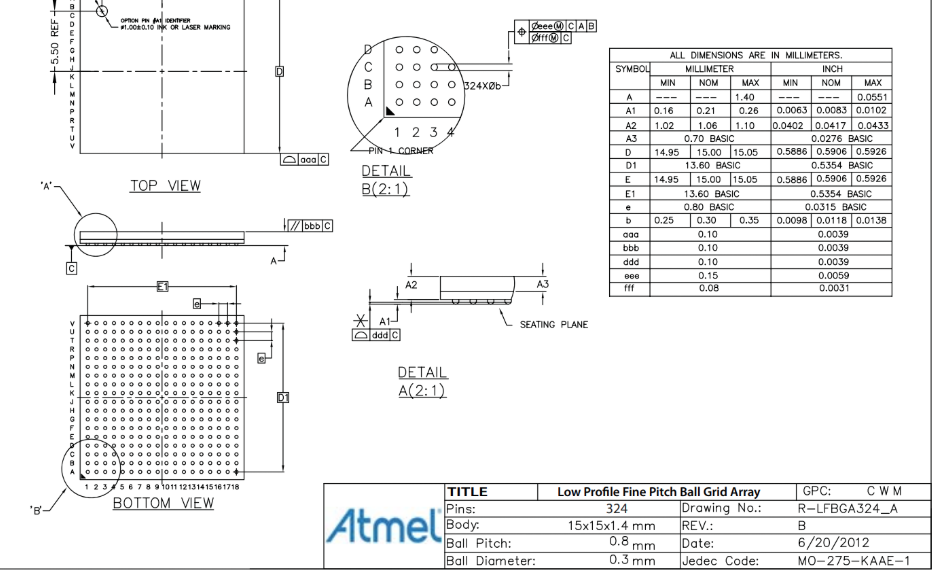
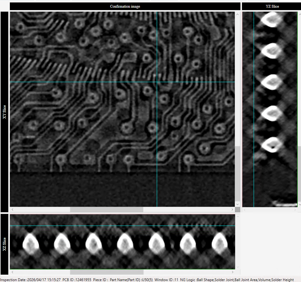
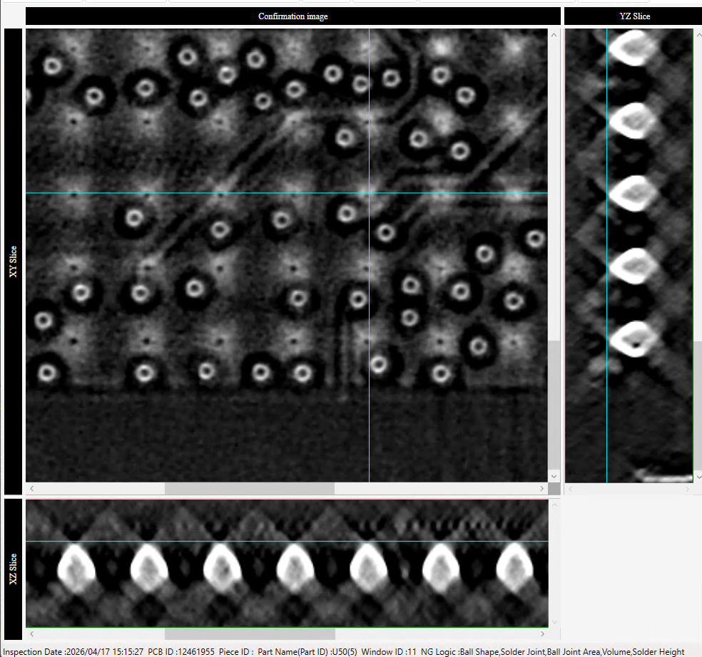
Hello, Yes, your assumption is correct. We are inspecting RMA boards returned from the customer and I programmed this BGA to fail every ball location intentionally. I have another question about the same BGA. Average ball height is around `200 microns, the data sheet for this part has 0.21 mm for the seating plane (A1). [cid:8f901b99-54d9-40b7-9f0e-81450a5949d8] The bottom of the BGA is multilayered. Please advise on the images bellow, I think the solder is penetrating the part internal structure. The images are the same cross section moving from the part down to the PCB: BGA internal layer, 3rd from bottom of the part [cid:466ed942-4d44-463e-b5a6-11d1b9d3319b] BGA internal 3rd layer to 2nd layer transition [cid:d0467a82-1a6a-41f4-b616-fb58f0b5b498] BGA 2nd internal layer [cid:eadf476f-b60a-4bba-97a8-f2bd7011763e] BGA 1st internal layer [cid:af856059-b77e-42e0-a4e2-a908b518200e] BGA bottom pad layer [cid:ec4bc478-2fd4-444b-9612-51f35a28ba6b] PCB pad layer [cid:8f85b965-1f09-473c-ba4e-a48cf4cf2fb6] Tamas Fodor Process Engineer office: [phone] [cid:keylogo_208x50_bbd3eb93-6727-44fa-b710-bdda3b5dcba5.png] [cid:badge_ps_25_b443c943-8b12-4814-87e8-575bb98241a4.png] fax: [phone] 7015 55th Street North cell: [phone] Oakdale, MN 55128 [email] keytronic.com This e-mail message may contain confidential or legally privileged information and is intended only for the use of the intended recipient(s). Any unauthorized disclosure, dissemination, distribution, copying or the taking of any action in reliance on the information herein is prohibited. E-mails are not secure and cannot be guaranteed to be error free as they can be intercepted, amended, or contain viruses. Anyone who communicates with us by e-mail is deemed to have accepted these risks. Key Tronic Corporation is not responsible for errors or omissions in this message and denies any responsibility for any damage arising from the use of e-mail. Any opinion and other statement contained in this message and any attachment are solely those of the author and do not necessarily represent those of the company. ________________________________
C
CustomerCustomer reply | Apr 20, 2026 at 12:17 PM
Adding Teresa. Tamas Fodor Process Engineer office: [phone] [cid:keylogo_208x50_0ac9ea0f-7f9d-4ec3-a3c7-8bb6a21f2376.png] [cid:badge_ps_25_e44ba8f1-1394-4cd2-bc08-c4fc88dbb807.png] fax: [phone] 7015 55th Street North cell: [phone] Oakdale, MN 55128 [email] keytronic.com ________________________________
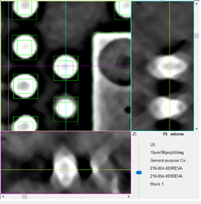
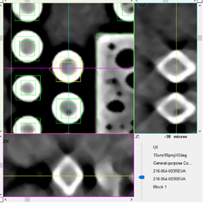
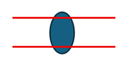
Hello Tamas, I'm not sure if this will answered you question, but below illustrates the true location of where the solder joint starts. I have some xray volume data examples of true HiP solder conditions, but not sure I can share them with due to there file size. I will try and send them to you email directly and see what happens. This slice layer above shows the shadow of the BGA solder joint lightly farther up into the BGA substrate, it is not. It is in fact a CT shadow of from the solder joint. This is likely the start of the solder bump / solder joint proper where it attached to the underside of the chip. This crude drawing shows the region where the true solder joint resides, above and below the red lines are the shadows. For most BGA the top tends to be pointer, then pad layer, but even at the level this is a small shadow.
C
CustomerCustomer reply | Apr 20, 2026 at 12:48 PM
Thank you for the information. I am wondering about the solder above the proper solder joint. Is it normal to see this much internally? Usually I don't see multiple layers, traces or vias before the bright tip of the solder balls. Tamas Fodor Process Engineer office: [phone] [cid:keylogo_208x50_bbd3eb93-6727-44fa-b710-bdda3b5dcba5.png] [cid:badge_ps_25_b443c943-8b12-4814-87e8-575bb98241a4.png] fax: [phone] 7015 55th Street North cell: [phone] Oakdale, MN 55128 [email] keytronic.com This e-mail message may contain confidential or legally privileged information and is intended only for the use of the intended recipient(s). Any unauthorized disclosure, dissemination, distribution, copying or the taking of any action in reliance on the information herein is prohibited. E-mails are not secure and cannot be guaranteed to be error free as they can be intercepted, amended, or contain viruses. Anyone who communicates with us by e-mail is deemed to have accepted these risks. Key Tronic Corporation is not responsible for errors or omissions in this message and denies any responsibility for any damage arising from the use of e-mail. Any opinion and other statement contained in this message and any attachment are solely those of the author and do not necessarily represent those of the company. ________________________________
Omron Application EngineerOmron reply | Apr 21, 2026 at 9:01 AM
Hello Tamas, Having the trace layers above the solder joints on BGAs is pretty normal. The BGA is questions' die is likely sitting on a moderately thick PCB substrate. In some instances you may need to alter the reconstruction values above and below PCB if the initial "Auto Creation" method is creating too much x-ray Z range in the image., it doesn't look like it in this case. We are seeing a fair amount of BTCs (BGA/LGA) components doing this. Its gets very interesting working on RF (WiFi, Bluetooth) modules where 200um --> 300um above the solder balls there are internal PCB with a double side mini board. The BGA package variant for these can become difficult to program, when they decided to go with the LGA variants it becomes even more complex to program, in this arrangement you are dealing with 100 - 250um thick solder joints, then the double sided internal components that often creates shadows or the software becomes unable to isolate the Z extraction slice layer to test as it keep try to jump of up to that internal layer of component instead of board pad level. So far the worst IMO are voltage regulators (DC/DC) I have programmed my fair share of the component from "Linear" and the issue is the same as previous component but now the internal components are copper coils, inductors, and caps, all the component types that block x-rays. of these the shadowing from the internal components then requires creating multiple individual settings (sub grouping) of pads with differing level of x-ray shadows.
C
CustomerCustomer reply | Apr 21, 2026 at 9:05 AM
Good morning, Thank you for the information. Can you confirm the last x-ray images I sent over look OK and it is not a defect? Tamas Fodor Process Engineer office: [phone] [cid:keylogo_208x50_bbd3eb93-6727-44fa-b710-bdda3b5dcba5.png] [cid:badge_ps_25_b443c943-8b12-4814-87e8-575bb98241a4.png] fax: [phone] 7015 55th Street North cell: [phone] Oakdale, MN 55128 [email] keytronic.com This e-mail message may contain confidential or legally privileged information and is intended only for the use of the intended recipient(s). Any unauthorized disclosure, dissemination, distribution, copying or the taking of any action in reliance on the information herein is prohibited. E-mails are not secure and cannot be guaranteed to be error free as they can be intercepted, amended, or contain viruses. Anyone who communicates with us by e-mail is deemed to have accepted these risks. Key Tronic Corporation is not responsible for errors or omissions in this message and denies any responsibility for any damage arising from the use of e-mail. Any opinion and other statement contained in this message and any attachment are solely those of the author and do not necessarily represent those of the company. ________________________________
freshdesk-inline-150152059712.png
1 tiny or repeated image hidden.
OA
Omron Application EngineerOmron reply | Apr 21, 2026 at 10:07 AM
Hello Tamas, I reviewed the latest images you provided and did not identify any defective balls. Francisco Villalpando Engineering Supervisor Direct: +[phone] [email]
C
CustomerCustomer reply | Apr 22, 2026 at 11:08 AM
Good morning, I am requesting remote assistance support to check an x-ray program BGA inspection. The settings are intentionally set to call out the BGA's, any advice to improve would be appreciated. The inspection is for 5 BGA's, we have a board where U50 is identified as a defect by one of our departments, but the x-ray inspections looks OK as far as I can tell. I have TeamViewer remote access credential for RVSX and the program is loaded with inspection tabulation data from the PCB in question. ID: 409332760 PSW: p9buhv53 Tamas Fodor Process Engineer office: [phone] [cid:keylogo_208x50_bbd3eb93-6727-44fa-b710-bdda3b5dcba5.png] [cid:badge_ps_25_b443c943-8b12-4814-87e8-575bb98241a4.png] fax: [phone] 7015 55th Street North cell: [phone] Oakdale, MN 55128 [email] keytronic.com This e-mail message may contain confidential or legally privileged information and is intended only for the use of the intended recipient(s). Any unauthorized disclosure, dissemination, distribution, copying or the taking of any action in reliance on the information herein is prohibited. E-mails are not secure and cannot be guaranteed to be error free as they can be intercepted, amended, or contain viruses. Anyone who communicates with us by e-mail is deemed to have accepted these risks. Key Tronic Corporation is not responsible for errors or omissions in this message and denies any responsibility for any damage arising from the use of e-mail. Any opinion and other statement contained in this message and any attachment are solely those of the author and do not necessarily represent those of the company. ________________________________
Hello Tamas, A quick follow up after remoting-in and taking a look at the BGA in question. The solder joints looked really good, it would be target if it wasn't for a handful of micro-voids. The thresholds you setup should be able to detect solder defects and are definitely very reasonable. If you add the few settings I made to: Surface Distance, Bridging Integration, offsetting the z slice for circularity inspection (2nd circularity group for pad interface) it will be a very robust test. Please be aware I did not copy the setting from pin A1 to the other pins.
C
CustomerCustomer reply | Apr 22, 2026 at 2:55 PM
Thank you, Ryan! Best regards, Tamas Tamas Fodor Process Engineer office: [phone] [cid:keylogo_208x50_bbd3eb93-6727-44fa-b710-bdda3b5dcba5.png] [cid:badge_ps_25_b443c943-8b12-4814-87e8-575bb98241a4.png] fax: [phone] 7015 55th Street North cell: [phone] Oakdale, MN 55128 [email] keytronic.com This e-mail message may contain confidential or legally privileged information and is intended only for the use of the intended recipient(s). Any unauthorized disclosure, dissemination, distribution, copying or the taking of any action in reliance on the information herein is prohibited. E-mails are not secure and cannot be guaranteed to be error free as they can be intercepted, amended, or contain viruses. Anyone who communicates with us by e-mail is deemed to have accepted these risks. Key Tronic Corporation is not responsible for errors or omissions in this message and denies any responsibility for any damage arising from the use of e-mail. Any opinion and other statement contained in this message and any attachment are solely those of the author and do not necessarily represent those of the company. ________________________________