A - AOI CASE ACK EN, A - 1 Hour Delay rslv, AOI - New CSAT Sent, LOCKED
Current case
Customer issue
Hello, The material of the pin you are seeing for the fiducial mark is made of steel. The boards are so small and have so many components on them, there isn't really a good point we can use other than the pin that goes through the board or a hollow oval shape towards the bottom. It won't even ley me set a Z- adjustment. I have adjusted the boxes, changed the settings for the mark, using the oval shape, and adjusted the thickness of the board multiple times just to see. Jessica Brothers 8702 Fairbanks North Houston Rd Houston, Texas 77064 PH: ([phone] Email: [email] PE EM AOI/SPI Engineer ⌘---------------------------------------------------------------------------------------------------------------------------------------------⌘ This email may contain confidential information and/or copyright material. This email is intended for the use of the addressee only. Any unauthorized use may be unlawful. If you receive this email by mistake, please advise the sender immediately by using the reply facility in your email software and delete this email. The integrity and security of this email cannot be guaranteed over the Internet. Therefore, it's advised for the receiver to verify the validity of this message with the sender. ⌘---------------------------------------------------------------------------------------------------------------------------------------------⌘ |---------+----------------------------> | | "AOI Tech Support| | | - US" | | | | | | | | | | | | | | | 08/04/2026 08:27 | | | AM | | | Please respond to| | | "AOI Tech Support| | | - US" | |---------+----------------------------> >--------------------------------------------------------------------------------------------------------------------------------------------------| | | | To: [email] | | cc: | | Subject: Re: Xray Image [Case: 1827612] | >--------------------------------------------------------------------------------------------------------------------------------------------------| Secret Level: |------------------------| | ( ) 1.Non-Confidential | | ( ) 2.Confidential | | ( ) 3.Secret | | ( ) 4.Top Secret | |------------------------| Priority Level: |--------------------| | ( ) 1.Normal | | ( ) 2.Urgent | | ( ) 3.Extra Urgent | |--------------------| ------------------------------------------------------------------------- Hello J-Jessica, Can you please tell use what is the fiduciary/board finish? From the photo it almost looks like there is solder on the top located fid. Without being able to actually take control of machine with board inside, I’m guessing that the system is having a difficult time reading the first fid due to its finish, and/or is searching within the adjustment window and finding the silver colored fixture. If there is solder on the fiducial, or uneven HASL finish is it going to be extremely difficult to setup a fid that is repeatable. My suggestion first would be to restrict the adjust window (search area) to be smaller, closer around the fid and avoiding the pallet surface. Then try and different combinations of fiducial setting and profiles from the dropdown inside adjustment window settings. Finally can you select one of the Z adjustment (laser points) components, test it, and tell me measure the machine displays. I want to rule out that maybe the board is not sitting too high up in pallet. On Fri, 31 Jul at 3:37 PM , J-Jessica Brothers wrote: Good afternoon, This is Jessica from Foxconn in Houston. I am trying to create a program and when I scan the board, the image comes out a little blurry. The program will not let me add components such as the Z adjustment to get started, the fiducial mark says extraction error and the splice image is solid white like it isn't picking up the image. I have tried multiple positions with two different carriers and changed the thickness several times. I have also tried changing the parameters to make it test OK and nothing. I am not sure how to fix this. Thank you for your time and attention. Jessica Brothers 8702 Fairbanks North Houston Rd Houston, Texas 77064 PH: ([phone] Email: [email] PE EM AOI/SPI Engineer ⌘---------------------------------------------------------------------------------------------------------------------------------------------⌘ This email may contain confidential information and/or copyright material. This email is intended for the use of the addressee only. Any unauthorized use may be unlawful. If you receive this email by mistake, please advise the sender immediately by using the reply facility in your email software and delete this email. The integrity and security of this email cannot be guaranteed over the Internet. Therefore, it's advised for the receiver to verify the validity of this message with the sender. ⌘---------------------------------------------------------------------------------------------------------------------------------------------⌘ 1827612:2549832
Conversation
Engineer and customer thread
17 messages
RM
Ryan MorrowOmron reply | Jul 30, 2026 at 2:23 PM
Hello Jessica, Can you please double check the board thickness value. This thickness value is for the PCB only, not fixture. To edit it go teach mode, maintain inspection program, select program, edit and check thickness.
AC
Andrew CrossleyOmron reply | Jul 30, 2026 at 2:25 PM
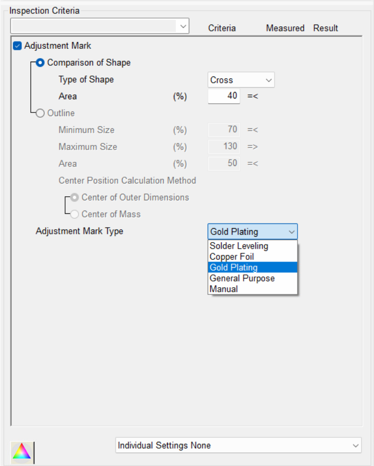
Hello Jessica, Is the X-Ray image blurry, or is the pcb overview image blurry? I think the first issue to take care of is the fiducial, since it may resolve the other errors as a result. Try changing the Adjustment Mark Type of the fiducials to something else as shown in the attached image. Thank you, Andrew Crossley
freshdesk-inline-150172139573.png
AC
Andrew CrossleyPrivate note | Jul 31, 2026 at 10:55 AM
Private
Merged from ticket 1826620 Subject: Re: Xray Image [Case: 1826383] Description: Hi, Yes, I did change the values multiple times. I used the PCB thickess, the carrier thickness, and some other numbers going above and below the values of each. Jessica Brothers 8702 Fairbanks North Houston Rd Houston, Texas 77064 PH: ([phone] Email: [email] PE EM AOI/SPI Engineer ⌘---------------------------------------------------------------------------------------------------------------------------------------------⌘ This email may contain confidential information and/or copyright material. This email is intended for the use of the addressee only. Any unauthorized use may be unlawful. If you receive this email by mistake, please advise the sender immediately by using the reply facility in your email software and delete this email. The integrity and security of this email cannot be guaranteed over the Internet. Therefore, it's advised for the receiver to verify the validity of this message with the sender. ⌘---------------------------------------------------------------------------------------------------------------------------------------------⌘ "AOI Tech Support - US" ---07/30/2026 01:24:17 PM---"AOI Tech Support - US" "AOI Tech Support - US" 07/30/2026 01:23 PM Please respond to "AOI Tech Support - US" To: [email] cc: Subject: Re: Xray Image [Case: 1826383] Secret Level: Priority Level: Hello Jessica, Can you please double check the board thickness value. This thickness value is for the PCB only, not fixture. To edit it go teach mode, maintain inspection program, select program, edit and check thickness. On Thu, 30 Jul at 1:02 PM , J-Jessica Brothers wrote: Good afternoon, This is Jessica from Foxconn in Houston. I am trying to create a program and when I scan the board, the image comes out a little blurry. The program will not let me add components such as the Z adjustment to get started, the fiducial mark says extraction error and the splice image is solid white like it isn't picking up the image. I have tried multiple positions with two different carriers and changed the thickness several times. I have also tried changing the parameters to make it test OK and nothing. I am not sure how to fix this. Thank you for your time and attention. Jessica Brothers 8702 Fairbanks North Houston Rd Houston, Texas 77064 PH: ([phone] Email: [email] PE EM AOI/SPI Engineer ⌘---------------------------------------------------------------------------------------------------------------------------------------------⌘ This email may contain confidential information and/or copyright material. This email is intended for the use of the addressee only. Any unauthorized use may be unlawful. If you receive this email by mistake, please advise the sender immediately by using the reply facility in your email software and delete this email. The integrity and security of this email cannot be guaranteed over the Internet. Therefore, it's advised for the receiver to verify the validity of this message with the sender. ⌘---------------------------------------------------------------------------------------------------------------------------------------------⌘ 1826383:2549832
3 tiny or repeated images hidden.
AC
Andrew CrossleyPrivate note | Jul 31, 2026 at 10:55 AM
Private
Tickets with IDs 1826620 and 1826621 are merged into this ticket.
AC
Andrew CrossleyPrivate note | Jul 31, 2026 at 10:55 AM
Private
Merged from ticket 1826621 Subject: Re: Xray Image [Case: 1826383] Description: Hi, Andrew. Yes, I did try changing all those settings as well. Jessica Brothers 8702 Fairbanks North Houston Rd Houston, Texas 77064 PH: ([phone] Email: [email] PE EM AOI/SPI Engineer ⌘---------------------------------------------------------------------------------------------------------------------------------------------⌘ This email may contain confidential information and/or copyright material. This email is intended for the use of the addressee only. Any unauthorized use may be unlawful. If you receive this email by mistake, please advise the sender immediately by using the reply facility in your email software and delete this email. The integrity and security of this email cannot be guaranteed over the Internet. Therefore, it's advised for the receiver to verify the validity of this message with the sender. ⌘---------------------------------------------------------------------------------------------------------------------------------------------⌘ "AOI Tech Support - US" ---07/30/2026 01:27:40 PM---"AOI Tech Support - US" "AOI Tech Support - US" 07/30/2026 01:25 PM Please respond to "AOI Tech Support - US" To: [email] cc: Subject: Re: Xray Image [Case: 1826383] Secret Level: Priority Level: Hello Jessica, Is the X-Ray image blurry, or is the pcb overview image blurry? I think the first issue to take care of is the fiducial, since it may resolve the other errors as a result. Try changing the Adjustment Mark Type of the fiducials to something else as shown in the attached image. Thank you, Andrew Crossley On Thu, 30 Jul at 1:02 PM , J-Jessica Brothers wrote: Good afternoon, This is Jessica from Foxconn in Houston. I am trying to create a program and when I scan the board, the image comes out a little blurry. The program will not let me add components such as the Z adjustment to get started, the fiducial mark says extraction error and the splice image is solid white like it isn't picking up the image. I have tried multiple positions with two different carriers and changed the thickness several times. I have also tried changing the parameters to make it test OK and nothing. I am not sure how to fix this. Thank you for your time and attention. Jessica Brothers 8702 Fairbanks North Houston Rd Houston, Texas 77064 PH: ([phone] Email: [email] PE EM AOI/SPI Engineer ⌘---------------------------------------------------------------------------------------------------------------------------------------------⌘ This email may contain confidential information and/or copyright material. This email is intended for the use of the addressee only. Any unauthorized use may be unlawful. If you receive this email by mistake, please advise the sender immediately by using the reply facility in your email software and delete this email. The integrity and security of this email cannot be guaranteed over the Internet. Therefore, it's advised for the receiver to verify the validity of this message with the sender. ⌘---------------------------------------------------------------------------------------------------------------------------------------------⌘ 1826383:2549832
3 tiny or repeated images hidden.
AC
Andrew CrossleyOmron reply | Jul 31, 2026 at 11:10 AM
Hello Jessica, Would you be able to provide us with some images of what you are seeing or allow remote access via Teams or Team Viewer to take a better look? Thank you, Andrew Crossley
AC
Andrew CrossleyPrivate note | Jul 31, 2026 at 5:10 PM
Private
Texted Jessica asking for a screenshot of the issue, but this may prove difficult due to site limitations with phones and pictures. I provided instructions for using the Window's snipping tool, and putting those images on the share drive so that she may email them from there.
AC
Andrew CrossleyPrivate note | Aug 3, 2026 at 2:12 PM
Private
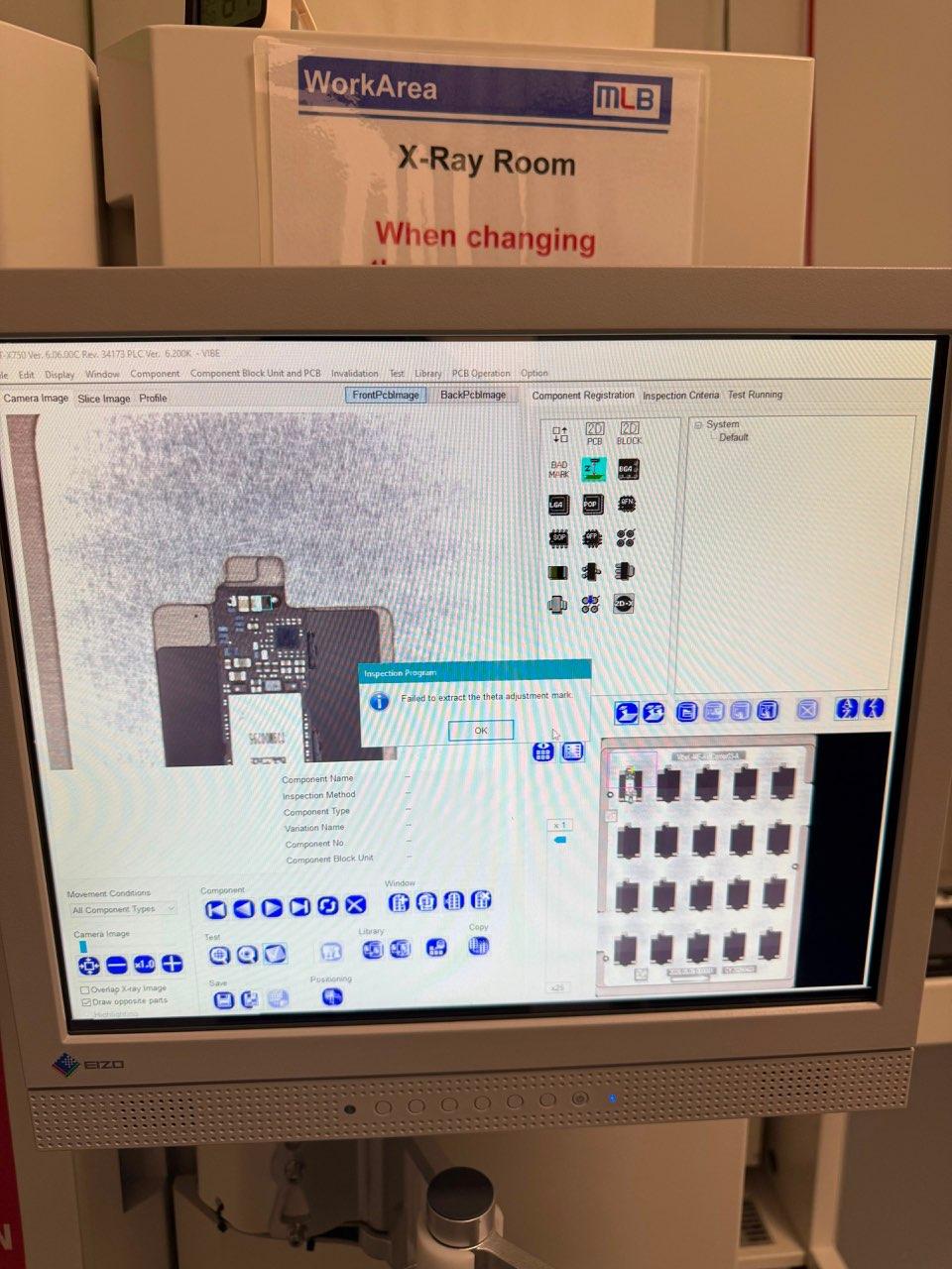
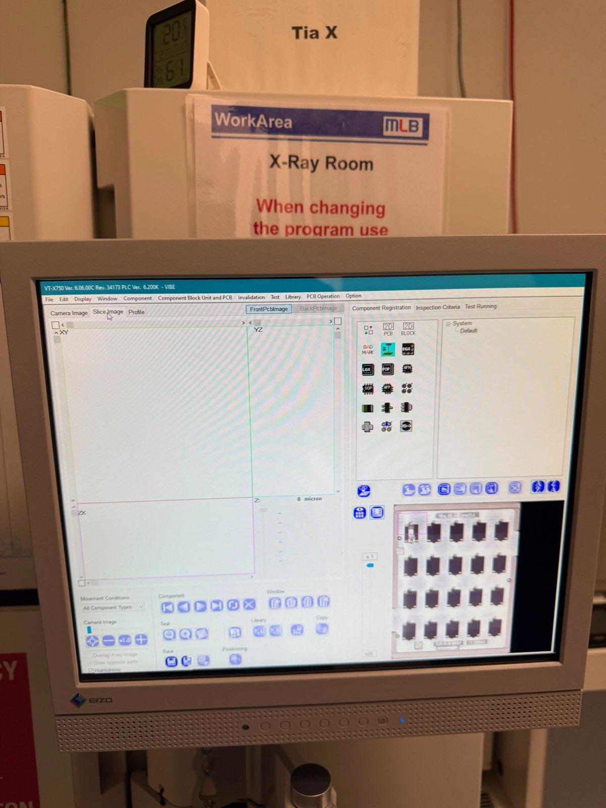
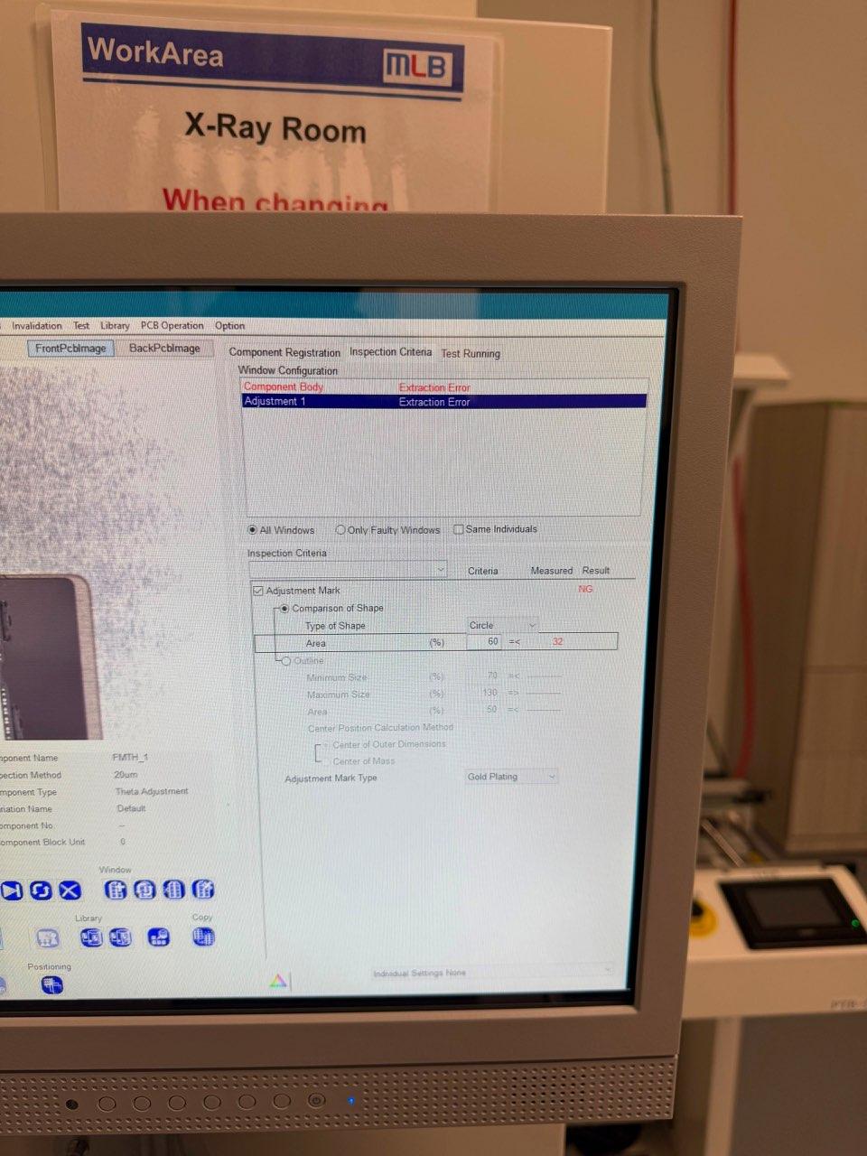
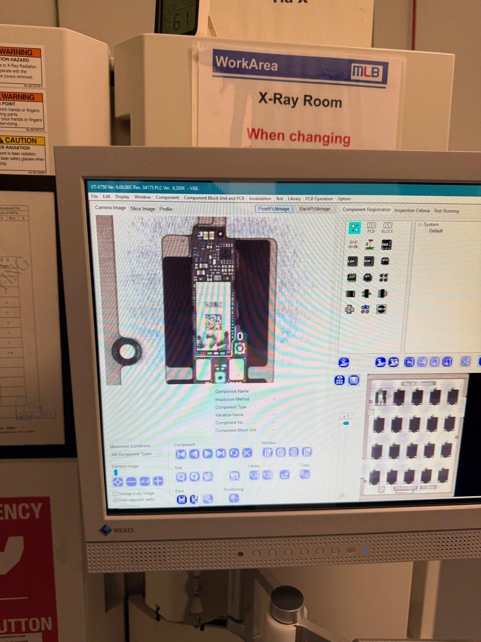
Attached are the images that were given to me today, depicting the issue Foxconn is having.
Hello J-Jessica, Can you please tell use what is the fiduciary/board finish? From the photo it almost looks like there is solder on the top located fid. Without being able to actually take control of machine with board inside, I’m guessing that the system is having a difficult time reading the first fid due to its finish, and/or is searching within the adjustment window and finding the silver colored fixture. If there is solder on the fiducial, or uneven HASL finish is it going to be extremely difficult to setup a fid that is repeatable. My suggestion first would be to restrict the adjust window (search area) to be smaller, closer around the fid and avoiding the pallet surface. Then try and different combinations of fiducial setting and profiles from the dropdown inside adjustment window settings. Finally can you select one of the Z adjustment (laser points) components, test it, and tell me measure the machine displays. I want to rule out that maybe the board is not sitting too high up in pallet.
FV
Francisco VillalpandoPrivate note | Aug 4, 2026 at 4:12 PM
Private
Tickets with IDs 1826383, 1827609, 1827611 and 1827613 are merged into this ticket.
FV
Francisco VillalpandoPrivate note | Aug 4, 2026 at 4:12 PM
Private
Merged from ticket 1826383 Subject: Xray Image Description: Good afternoon, This is Jessica from Foxconn in Houston. I am trying to create a program and when I scan the board, the image comes out a little blurry. The program will not let me add components such as the Z adjustment to get started, the fiducial mark says extraction error and the splice image is solid white like it isn't picking up the image. I have tried multiple positions with two different carriers and changed the thickness several times. I have also tried changing the parameters to make it test OK and nothing. I am not sure how to fix this. Thank you for your time and attention. Jessica Brothers 8702 Fairbanks North Houston Rd Houston, Texas 77064 PH: ([phone] Email: [email] PE EM AOI/SPI Engineer ⌘---------------------------------------------------------------------------------------------------------------------------------------------⌘ This email may contain confidential information and/or copyright material. This email is intended for the use of the addressee only. Any unauthorized use may be unlawful. If you receive this email by mistake, please advise the sender immediately by using the reply facility in your email software and delete this email. The integrity and security of this email cannot be guaranteed over the Internet. Therefore, it's advised for the receiver to verify the validity of this message with the sender. ⌘---------------------------------------------------------------------------------------------------------------------------------------------⌘
FV
Francisco VillalpandoPrivate note | Aug 4, 2026 at 4:12 PM
Private
Merged from ticket 1827609 Subject: Re: Xray Image [Case: 1826383] Description: Yes, I can setup a webex call and you can remote in that way. I cannot do any pictures though. If that works for you, what time would be good? Jessica Brothers 8702 Fairbanks North Houston Rd Houston, Texas 77064 PH: ([phone] Email: [email] PE EM AOI/SPI Engineer ⌘---------------------------------------------------------------------------------------------------------------------------------------------⌘ This email may contain confidential information and/or copyright material. This email is intended for the use of the addressee only. Any unauthorized use may be unlawful. If you receive this email by mistake, please advise the sender immediately by using the reply facility in your email software and delete this email. The integrity and security of this email cannot be guaranteed over the Internet. Therefore, it's advised for the receiver to verify the validity of this message with the sender. ⌘---------------------------------------------------------------------------------------------------------------------------------------------⌘ "AOI Tech Support - US" ---07/31/2026 10:13:16 AM---"AOI Tech Support - US" "AOI Tech Support - US" 07/31/2026 10:10 AM Please respond to "AOI Tech Support - US" To: [email] cc: Subject: Re: Xray Image [Case: 1826383] Secret Level: Priority Level: Hello Jessica, Would you be able to provide us with some images of what you are seeing or allow remote access via Teams or Team Viewer to take a better look? Thank you, Andrew Crossley On Thu, 30 Jul at 1:25 PM , AOI Tech Support - US wrote: Hello Jessica, Is the X-Ray image blurry, or is the pcb overview image blurry? I think the first issue to take care of is the fiducial, since it may resolve the other errors as a result. Try changing the Adjustment Mark Type of the fiducials to something else as shown in the attached image. Thank you, Andrew Crossley On Thu, 30 Jul at 1:02 PM , J-Jessica Brothers wrote: Good afternoon, This is Jessica from Foxconn in Houston. I am trying to create a program and when I scan the board, the image comes out a little blurry. The program will not let me add components such as the Z adjustment to get started, the fiducial mark says extraction error and the splice image is solid white like it isn't picking up the image. I have tried multiple positions with two different carriers and changed the thickness several times. I have also tried changing the parameters to make it test OK and nothing. I am not sure how to fix this. Thank you for your time and attention. Jessica Brothers 8702 Fairbanks North Houston Rd Houston, Texas 77064 PH: ([phone] Email: [email] PE EM AOI/SPI Engineer ⌘---------------------------------------------------------------------------------------------------------------------------------------------⌘ This email may contain confidential information and/or copyright material. This email is intended for the use of the addressee only. Any unauthorized use may be unlawful. If you receive this email by mistake, please advise the sender immediately by using the reply facility in your email software and delete this email. The integrity and security of this email cannot be guaranteed over the Internet. Therefore, it's advised for the receiver to verify the validity of this message with the sender. ⌘---------------------------------------------------------------------------------------------------------------------------------------------⌘ 1826383:2549832
3 tiny or repeated images hidden.
FV
Francisco VillalpandoPrivate note | Aug 4, 2026 at 4:12 PM
Private
Merged from ticket 1827611 Subject: Re: Xray Image [Case: 1826383] Description: Hi, Andrew. Yes, I did try changing all those settings as well. Jessica Brothers 8702 Fairbanks North Houston Rd Houston, Texas 77064 PH: ([phone] Email: [email] PE EM AOI/SPI Engineer ⌘---------------------------------------------------------------------------------------------------------------------------------------------⌘ This email may contain confidential information and/or copyright material. This email is intended for the use of the addressee only. Any unauthorized use may be unlawful. If you receive this email by mistake, please advise the sender immediately by using the reply facility in your email software and delete this email. The integrity and security of this email cannot be guaranteed over the Internet. Therefore, it's advised for the receiver to verify the validity of this message with the sender. ⌘---------------------------------------------------------------------------------------------------------------------------------------------⌘ "AOI Tech Support - US" ---07/30/2026 01:27:40 PM---"AOI Tech Support - US" "AOI Tech Support - US" 07/30/2026 01:25 PM Please respond to "AOI Tech Support - US" To: [email] cc: Subject: Re: Xray Image [Case: 1826383] Secret Level: Priority Level: Hello Jessica, Is the X-Ray image blurry, or is the pcb overview image blurry? I think the first issue to take care of is the fiducial, since it may resolve the other errors as a result. Try changing the Adjustment Mark Type of the fiducials to something else as shown in the attached image. Thank you, Andrew Crossley On Thu, 30 Jul at 1:02 PM , J-Jessica Brothers wrote: Good afternoon, This is Jessica from Foxconn in Houston. I am trying to create a program and when I scan the board, the image comes out a little blurry. The program will not let me add components such as the Z adjustment to get started, the fiducial mark says extraction error and the splice image is solid white like it isn't picking up the image. I have tried multiple positions with two different carriers and changed the thickness several times. I have also tried changing the parameters to make it test OK and nothing. I am not sure how to fix this. Thank you for your time and attention. Jessica Brothers 8702 Fairbanks North Houston Rd Houston, Texas 77064 PH: ([phone] Email: [email] PE EM AOI/SPI Engineer ⌘---------------------------------------------------------------------------------------------------------------------------------------------⌘ This email may contain confidential information and/or copyright material. This email is intended for the use of the addressee only. Any unauthorized use may be unlawful. If you receive this email by mistake, please advise the sender immediately by using the reply facility in your email software and delete this email. The integrity and security of this email cannot be guaranteed over the Internet. Therefore, it's advised for the receiver to verify the validity of this message with the sender. ⌘---------------------------------------------------------------------------------------------------------------------------------------------⌘ 1826383:2549832
3 tiny or repeated images hidden.
FV
Francisco VillalpandoPrivate note | Aug 4, 2026 at 4:12 PM
Private
Merged from ticket 1827613 Subject: Re: Xray Image [Case: 1826383] Description: Hi, Yes, I did change the values multiple times. I used the PCB thickess, the carrier thickness, and some other numbers going above and below the values of each. Jessica Brothers 8702 Fairbanks North Houston Rd Houston, Texas 77064 PH: ([phone] Email: [email] PE EM AOI/SPI Engineer ⌘---------------------------------------------------------------------------------------------------------------------------------------------⌘ This email may contain confidential information and/or copyright material. This email is intended for the use of the addressee only. Any unauthorized use may be unlawful. If you receive this email by mistake, please advise the sender immediately by using the reply facility in your email software and delete this email. The integrity and security of this email cannot be guaranteed over the Internet. Therefore, it's advised for the receiver to verify the validity of this message with the sender. ⌘---------------------------------------------------------------------------------------------------------------------------------------------⌘ "AOI Tech Support - US" ---07/30/2026 01:24:17 PM---"AOI Tech Support - US" "AOI Tech Support - US" 07/30/2026 01:23 PM Please respond to "AOI Tech Support - US" To: [email] cc: Subject: Re: Xray Image [Case: 1826383] Secret Level: Priority Level: Hello Jessica, Can you please double check the board thickness value. This thickness value is for the PCB only, not fixture. To edit it go teach mode, maintain inspection program, select program, edit and check thickness. On Thu, 30 Jul at 1:02 PM , J-Jessica Brothers wrote: Good afternoon, This is Jessica from Foxconn in Houston. I am trying to create a program and when I scan the board, the image comes out a little blurry. The program will not let me add components such as the Z adjustment to get started, the fiducial mark says extraction error and the splice image is solid white like it isn't picking up the image. I have tried multiple positions with two different carriers and changed the thickness several times. I have also tried changing the parameters to make it test OK and nothing. I am not sure how to fix this. Thank you for your time and attention. Jessica Brothers 8702 Fairbanks North Houston Rd Houston, Texas 77064 PH: ([phone] Email: [email] PE EM AOI/SPI Engineer ⌘---------------------------------------------------------------------------------------------------------------------------------------------⌘ This email may contain confidential information and/or copyright material. This email is intended for the use of the addressee only. Any unauthorized use may be unlawful. If you receive this email by mistake, please advise the sender immediately by using the reply facility in your email software and delete this email. The integrity and security of this email cannot be guaranteed over the Internet. Therefore, it's advised for the receiver to verify the validity of this message with the sender. ⌘---------------------------------------------------------------------------------------------------------------------------------------------⌘ 1826383:2549832
3 tiny or repeated images hidden.
FV
Francisco VillalpandoPrivate note | Aug 4, 2026 at 5:00 PM
Private
Tickets with IDs 1827612 is merged into this ticket.
FV
Francisco VillalpandoPrivate note | Aug 4, 2026 at 5:00 PM
Private
Merged from ticket 1827612 Subject: Xray Image Description: Good afternoon, This is Jessica from Foxconn in Houston. I am trying to create a program and when I scan the board, the image comes out a little blurry. The program will not let me add components such as the Z adjustment to get started, the fiducial mark says extraction error and the splice image is solid white like it isn't picking up the image. I have tried multiple positions with two different carriers and changed the thickness several times. I have also tried changing the parameters to make it test OK and nothing. I am not sure how to fix this. Thank you for your time and attention. Jessica Brothers 8702 Fairbanks North Houston Rd Houston, Texas 77064 PH: ([phone] Email: [email] PE EM AOI/SPI Engineer ⌘---------------------------------------------------------------------------------------------------------------------------------------------⌘ This email may contain confidential information and/or copyright material. This email is intended for the use of the addressee only. Any unauthorized use may be unlawful. If you receive this email by mistake, please advise the sender immediately by using the reply facility in your email software and delete this email. The integrity and security of this email cannot be guaranteed over the Internet. Therefore, it's advised for the receiver to verify the validity of this message with the sender. ⌘---------------------------------------------------------------------------------------------------------------------------------------------⌘
OA
Omron Application EngineerOmron reply | Aug 6, 2026 at 6:24 PM