XT750 – LGA HiP Visibility & Multi‑Slice Inspection
CustomerNot indexed
CompanyNot indexed
Priority2
TypeFYI-No Action Required
UpdatedApr 24, 2026 at 12:30 PM
Thread4 messages
Ticket metadata
Group
AOI US (150000419797)
Status
Closed (5)
Created
Apr 2, 2026 at 4:30 PM
Requester
Not indexed
Company
Not indexed
Last synced
Aug 2, 2026 at 11:14 PM
Resolved
Apr 14, 2026 at 8:56 AM
Closed
Apr 22, 2026 at 12:26 PM
Tags
A - AOI CASE ACK EN, A - Reply Open, A - 1 Hour Delay rslv, AOI - New CSAT Sent, LOCKED
Current case
Customer issue
Hello Omron Support Team, We are requesting guidance on optimizing our Omron XT750 X‑ray inspection to detect possible Head‑in‑Pillow defects related to oxidation on an LGA component, MPN LBAD0XX1SC‑005. Currently, the standard inspection slice does not clearly show the solder connection for this device. We are unable to reliably differentiate the PCB pad, solder layer, and LGA land interface, even though results indicate potential HiP‑type separation. We would like to understand if the XT750 supports a multi‑slice or multi‑layer inspection approach, where different slice depths or image settings can be used to separately emphasize the pad, solder, and component interface in order to better evaluate solder wetting. We are also interested in your recommendation on whether slice inspection is appropriate for LGA HiP detection, or if oblique (tilt) imaging is preferred, along with any suggested parameter settings or inspection algorithms for this application. Any reference settings, application notes, or examples related to LGA HiP inspection would be appreciated. An image of the component and the datasheet are attached for reference. Thank you for your support. Sarah Cerna Process Technician - PCBA Star Precision, LP 11236 Brittmoore Park Dr | Houston , TX 77041 Main: 5410 Brystone Dr | Houston, TX 77041 T: ([phone] F: ([phone] [email] | www.star-precision.com Fabrication I Machining I Electronics I ISO 9001:2015 This e-mail, including any attached files, may contain confidential and privileged information and is intended for the addressee(s) only. If you are not the intended recipient please notify the originator and delete the email immediately. The unauthorized review, use, distribution, or disclosure by others is strictly prohibited. Any views or opinions presented in this email are solely those of the author and do not necessarily represent those of the company. Finally, the recipient should check this email and any attachments for the presence of viruses. The company accepts no liability for any damage caused by any virus transmitted by this email.
Hello Sarah, Just so we are on the same page, this component is actually an LGA, without solder bumps on component correct? Here are some tip that may help. 1. Do not use LGA family to set this component up. Please use General Purpose Component. 2. Please ensure there is as little board warpage as possible, what you want to avoid is one pad being clear and the other corner out of focus. 3. Draw the X/Y area of the position range window bigger than the component by a small margin. 4. When setting up the "Reconstruction Above/Below PCB" for above I would try to only select high enough that the solder joint are just starting to blur out, any higher then the system my try and track the components inside of LGA body. 5. Verify that the Z-extraction is working properly. Click on Z offset and perform a window test. The part should be focusing on the pad/solder interface, if it is just a little off add a +- offset to move there. If it is way off then either reduce the "Reconstruction above PCB" a little or start adding projection or x-ray power to overcome the noise. 6. Once the Z-extraction is stable verity X/Y adjust is functioning properly. Click on min. bin. thres. under X/Y adjust thresholds, then perform window test. You want to see only the solder joint having white overlay. If noisy up the min.. bin. threshold to accomadate. 7. Set the "Matching" score accordingly, should be in the 30-40%s, if that is the case set limit to 20%-30%.\ 8. Setup common settings min. bin. thresholds so it binarizing the wetted solder properly. 9. I would setup: Solder Area, Solder Shape, Bridging, and optionally you could setup Brightness/Wettablity test, specifically the Brightness min/max.
C
CustomerCustomer reply | Apr 8, 2026 at 12:22 PM
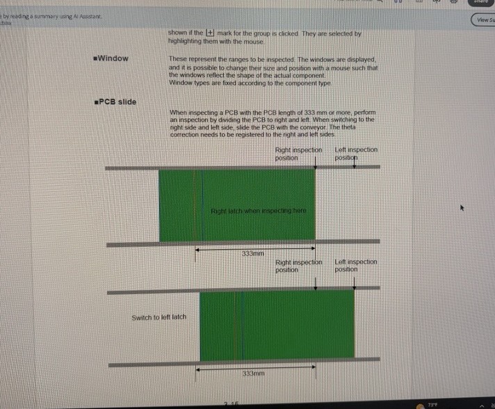
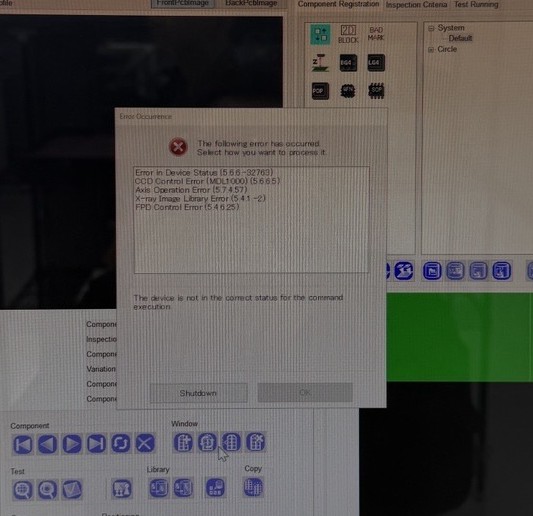
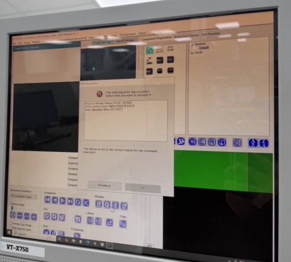
Hello Omron Support, Thank you for the suggestion. It significantly improved visibility of the LGA solder connections. I have another issue I would like assistance with. I attempted to create an inspection program for a PCB measuring 173.86 mm × 492.6 mm. Based on the manuals, I followed the procedure for capturing images of boards exceeding 333 mm in length. However, once the PCB image scan completes, multiple system errors occur, forcing a shutdown. Attached are screenshots of the error messages and the relevant manual section. Is there additional documentation related to large-board imaging, or are there known limitations or recommended settings for boards of this size? Any alternative approaches or suggestions would be appreciated. Best regards, Sarah Cerna Process Technician - PCBA Star Precision, LP 11236 Brittmoore Park Dr | Houston , TX 77041 Main: 5410 Brystone Dr | Houston, TX 77041 T: ([phone] F: ([phone] [email] | www.star-precision.com Fabrication I Machining I Electronics I ISO 9001:2015 This e-mail, including any attached files, may contain confidential and privileged information and is intended for the addressee(s) only. If you are not the intended recipient please notify the originator and delete the email immediately. The unauthorized review, use, distribution, or disclosure by others is strictly prohibited. Any views or opinions presented in this email are solely those of the author and do not necessarily represent those of the company. Finally, the recipient should check this email and any attachments for the presence of viruses. The company accepts no liability for any damage caused by any virus transmitted by this email.
PCB Slide.jpgX-Ray Error Message after PCB Image creation.jpgX-Ray Error Message.jpg7a519e58c4cf6ff0f1c35fd4e1aa3c50_artboard1copy.png
C
CustomerCustomer reply | Apr 8, 2026 at 12:59 PM
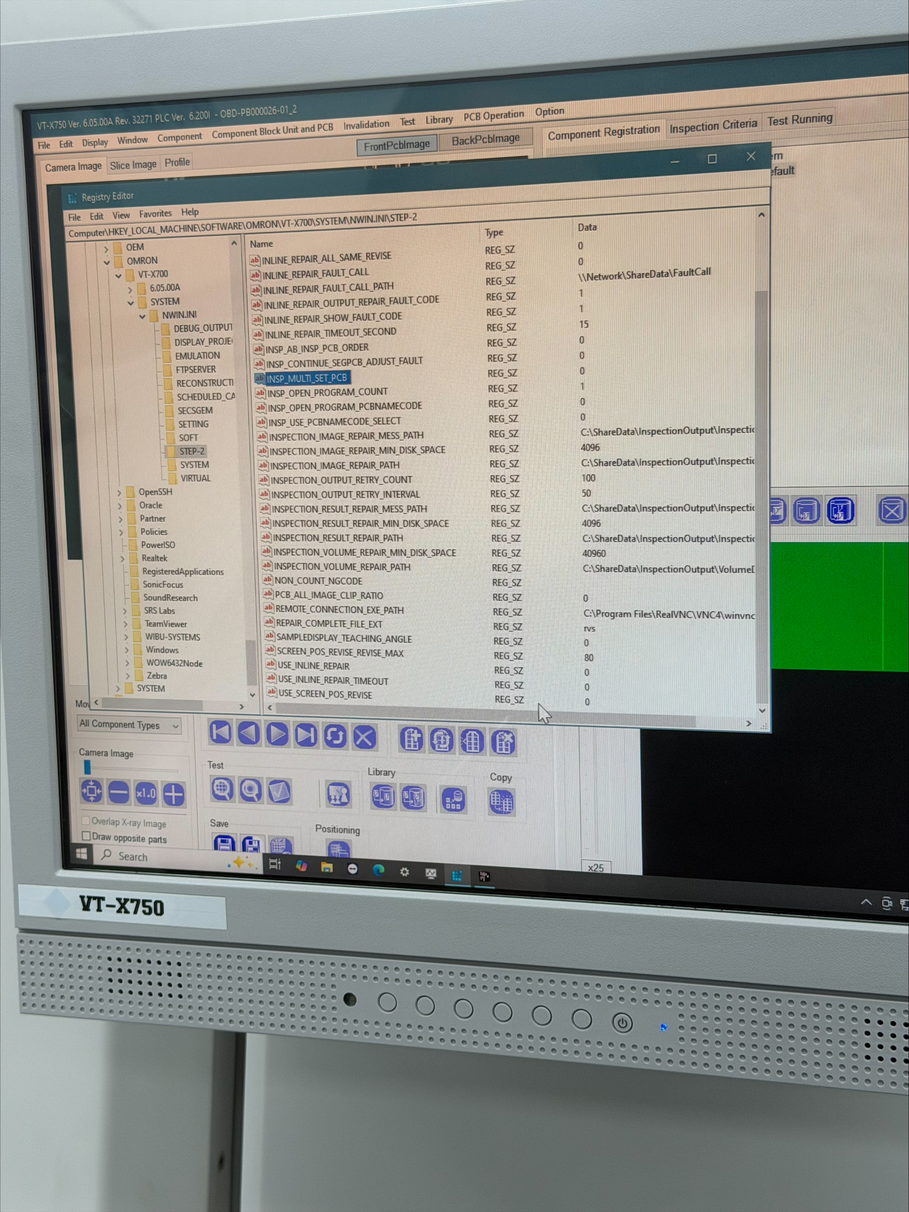
Hello Omron Support Team, I wanted to provide an update on our end. We were able to access the system settings and change the insp_multi_set_pcb variable from 0 to 1, then re‑initialize the X‑ray software. After doing so, we were successful in creating the PCB Slide image for the inspection program. Before proceeding further, we wanted to check with you: would changing this setting have any impact on inspection behavior, image reconstruction, or inspection results that we should be aware of? If there are any known side effects or recommendations when using this setting, please let us know. Thank you for your continued support. Best regards, Sarah Cerna Process Technician - PCBA Star Precision, LP 11236 Brittmoore Park Dr | Houston , TX 77041 Main: 5410 Brystone Dr | Houston, TX 77041 T: ([phone] F: ([phone] [email] | www.star-precision.com Fabrication I Machining I Electronics I ISO 9001:2015 This e-mail, including any attached files, may contain confidential and privileged information and is intended for the addressee(s) only. If you are not the intended recipient please notify the originator and delete the email immediately. The unauthorized review, use, distribution, or disclosure by others is strictly prohibited. Any views or opinions presented in this email are solely those of the author and do not necessarily represent those of the company. Finally, the recipient should check this email and any attachments for the presence of viruses. The company accepts no liability for any damage caused by any virus transmitted by this email.